
We designed a fully functional alarm clock for our 2nd semester lab project at the Department of of Electronics and Telecommunication Engineering at University of Moratuwa, Sri Lanka.
Our objective was to design and implement an alarm clock that offer the functionality to set time and date, set alarms throughout the day with the features of delete, change, and select an alarm tone for each alarm. The alarm clock should provide a user friendly interface using a keypad and an LCD. The project was completed in two stages. During the first stage, each team member developed a stand-alone microproduct corresponding to a different subsystem of the alarm clock.
- Alarm Timing
- Audio Output
- Key Input
- Menu Display
During this stage, the algorithms for each subsystem were developed and tested using code written in Arduino C++ and simulated in both Proteus software platform and on the breadboard. Next, the firmware for each subsystem was developed in AVR C++ for ATMega644P microcontroller. Functions were written, for each task that contributes to the final product and compiled into a header file that would later be combined to develop the final algorithm. The development of the Alarm Timing microproduct is explained in detail in this blog post.
Firmware Development
The firmware was developed in Microchip Studio for ATMega644P microcontroller. A keypad was used to take number inputs from the user and an LCD was used to display the user interface of the clock. A sound system comprised of a buzzer was used to generate sounds for the alarms. The alarm clock keeps track of time and date using the RTC IC DS3231 which communicates with the microcontroller through the I2C interface.
The following functions were developed by each member in their own microproduct. They were compiled into separate header files.

The final algorithm was developed by Chathuni Wijegunawardana based on the above header files. This algorithm provided a menu navigation system for the user to access each function. The inputs were taken using a 4×3 keypad and 2 main push buttons. The push buttons’ functionalities were Menu and Stop alarm. After accessing the menu by the Menu button, the navigation and number inputs were taken using the keypad. The final algorithm is illustrated in the following flow chart.
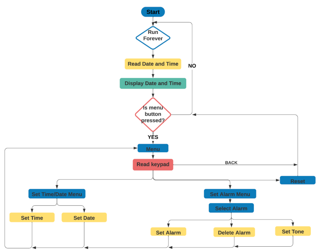
The alarm offered the user to set 6 different alarms with a desired tone for each of them. The checks for alarm times were implemented using software interrupts. The reason for using interrupts was to detect alarms even when the user is in the middle of the menu. The Timer Overflow Interrupt of 16-bit Timer/Counter 1 of ATMega644P was used in this case. The interrupt service routine (ISR) was written to iterate through each alarm in the alarm list and check whether the time is equal to any of the active alarms. If found, its ring function will be called.
Between the menu, an error message was programmed to be displayed whenever the user entered an invalid input.
The AVR C++ codes of the firmware of the alarm clock can be found at the following Firmware Google Drive link.
The algorithm was tested on Proteus Simulation software.
Schematic Design
The schematic diagram was finalized by combining each sub-schematic from the microproducts. The final schematic was designed by Dilani Widanapathiranage using Altium software.
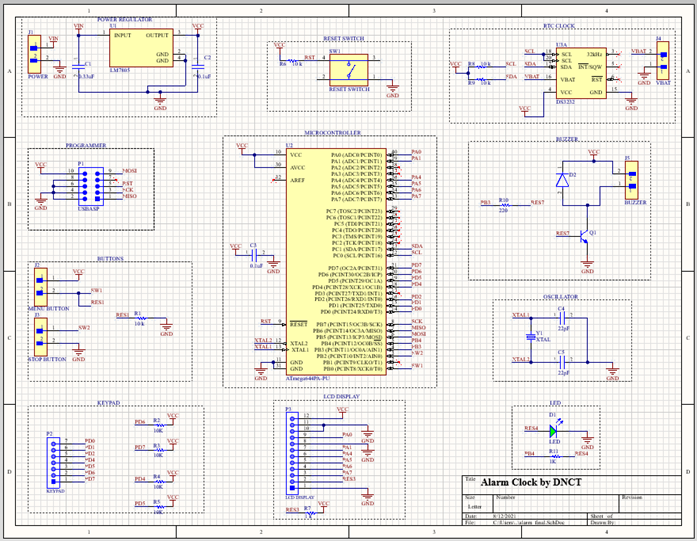
The elements in the PCB is as follows.
- Microcontroller – ATMega644P
- 5V Regulator – LM7805
- DS3231 Real Time Clock IC
- 16MHz Oscillator
- Buzzer and supporting components
- Programming Header for USBASP
- Headers for LCD and Keypad Interfacing
- Menu and Stop Alarm Push Buttons
Bypass capacitors were added according to the datasheets of the components wherever required.
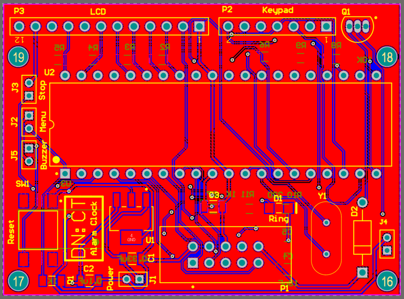
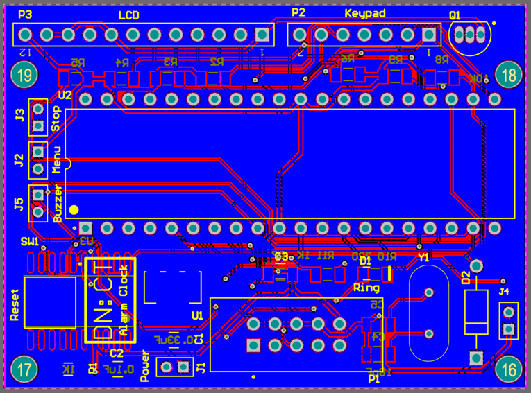
PCB Layout Design
The PCB layout was designed using Altium by Dilani Widanapathiranage and Chathuni Wijegunawardana. Several practical design aspects were taken into consideration when the components are being placed and routed.
- Reducing the form factor
- Neatness
- Minimizing the lengths of routing paths
- Placing bypass capacitors near the microcontroller according to datasheet guidelines
- Minimized routing below the microcontroller and avoiding routing below voltage regulator and oscillator
- Same value resistors were placed as blocks for the convenience of soldering
- Labels were added to all components with their values for the convenience of soldering
- Headers and connectors placed close to the edges of the PCB for the convenience of connecting wires
The PCB layout is illustrated below.

The 3D visualization of the PCB is shown below.
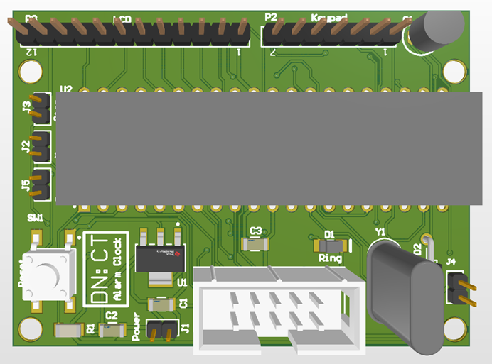
The dimensions of the final PCB were 61.6 mm x 45.3 mm.
The Altium Project folder of the PCB can be accessed through this PCB Google Drive link.
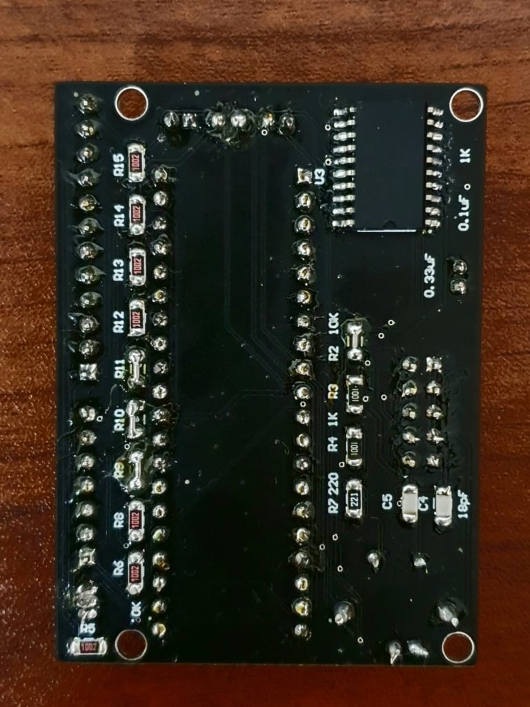
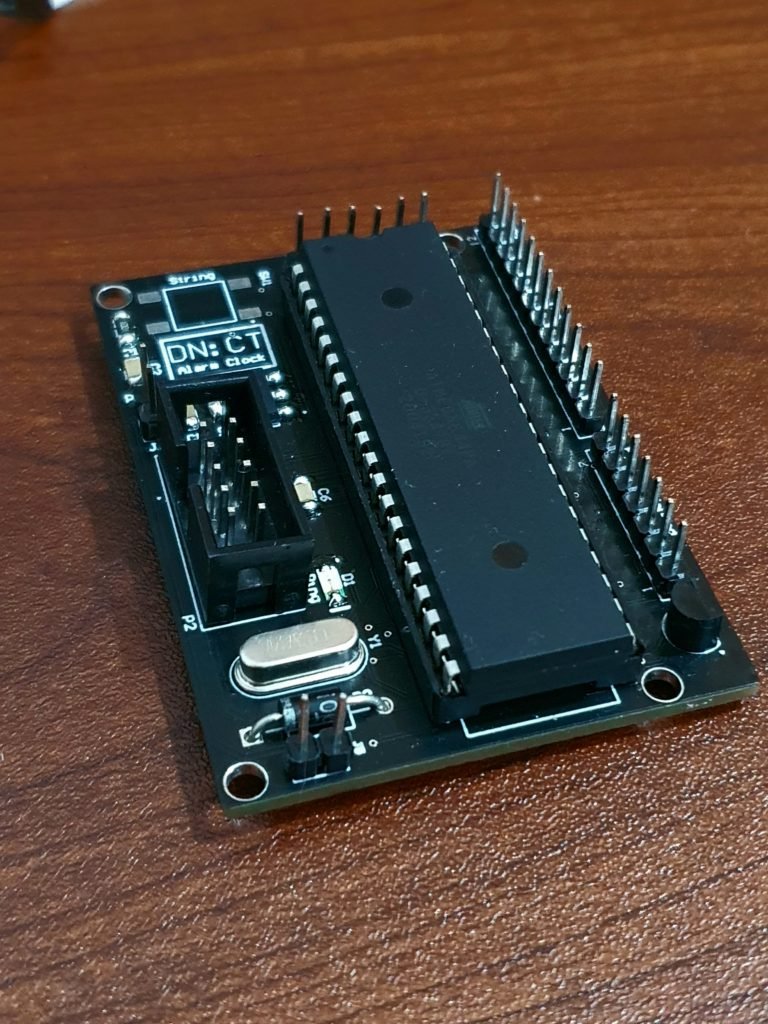
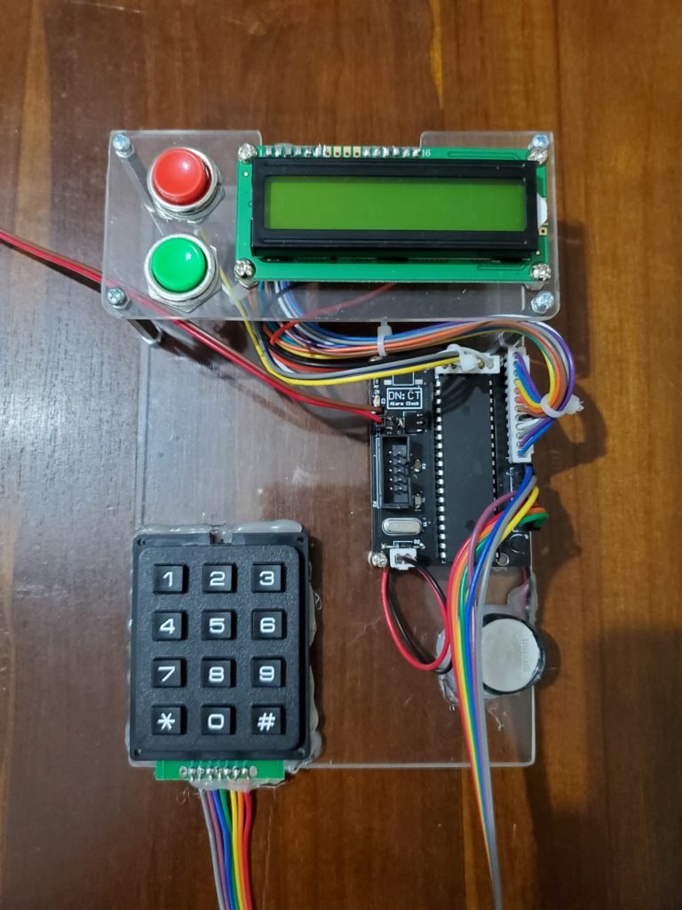
Fabricated PCB
The designed PCB was manufactured from JLCPCB. The components were ordered from Arrow Electronics and were hand soldered by Pahan Mendis.
First, the SMD components on the bottom side and then the top side were soldered onto the PCB using 0.635mm(0.025″) solder wire and the conical tip. Then the through-hole components were soldered using 0.8mm solder wire and the chisel tip.
The fabricated PCB is shown below.

Prototype
A prototype was created using the following components to demonstrate the correct functionality.
- Fabricated PCB
- LCD
- 4×3 Keypad
- 2 Push Buttons
- Coin-cell Battery
- DC Power Supply
- Buzzer
The video demonstration of the correct implementation is below.
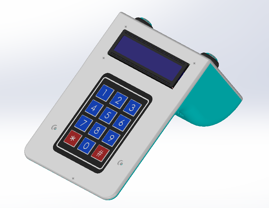
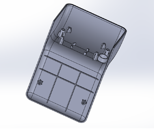
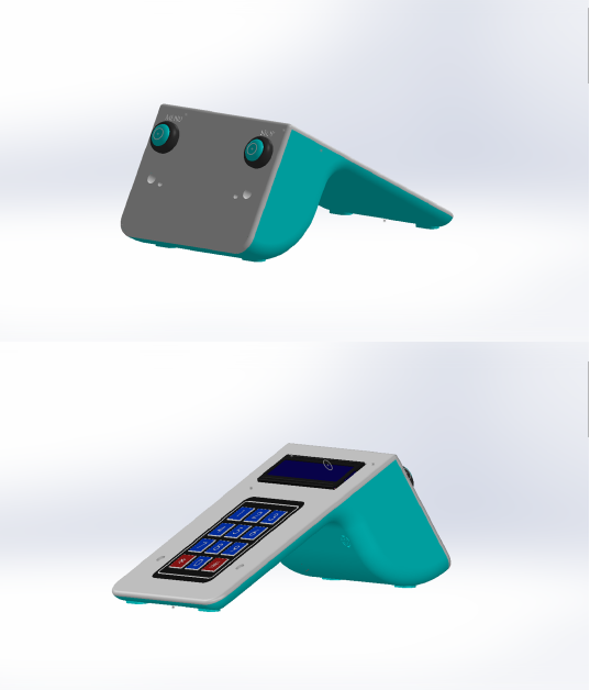
Enclosure Design
An ergonomic enclosure was designed for the final product by Nima Wickramasinghe with the help of Thilanka Widanagamage using Solidworks. This enclosure integrated the following components within its design.
- PCB
- LCD
- Keypad
- 4 AAA Battery Pack
- CR2032 Coin-cell Battery
- 2 Push Buttons
- Buzzer
Our aim was to create an enclosure that would have the necessary strength for day to day use. It should also have the requirements to be easily opened for repairs and maintenance while having a very unique and aesthetic design.
The enclosure was split into 2 separate parts.
Bottom Part
The bottom part gets connected to the top part using four mounting bosses. Also, lips and grooves are etched onto the edges where the two parts meet. It also contains ribs for additional support and high strength. It also helps to maintain shape under high-stress conditions. The bottom part houses the coin cell battery, PCB, and the buzzer. We created a separate slot to accommodate the coin cell battery. The PCB is mounted on 4 mounting bosses. A circular slot is separately carved to accommodate the buzzer. A vent is created on the bottom side to pass the sound of the buzzer outside. 4 straight slots are etched onto the bottom surface, where rubber pads will be attached later on. The rubber pads on the bottom will help stabilize the product and help stop slipping.
Top Part
The top part too includes the required mounting bosses to connect to the bottom part along with the lips and grooves. It houses the 4×3 matrix keypad, LCD, 4xAAA battery holder, and the two momentary switches. Separate holes are cut out for the momentary switches to be attached. The holes have a carving above them so that the user can easily identify the function of the switch. A 1mm depth slot is carved out in the front face to accommodate the 4×3 matrix keypad. A small slot is cut at the bottom to get the wires inside the enclosure. A large window is cut at the top part of the front face for the LCD screen. Also a large slot is created at the back to accommodate the 4XAAA battery holder. It also contains the holes required to attach the cover of the battery compartment.

The final enclosure design is illustrated below.
The Solidworks design folder can be accessed through Enclosure Google Drive link.
Conclusion
The project was successfully completed under the supervision and guidance of Mr.Kithmin Wickramasinghe and Mr.Abarajithan Gnaneswaran, Junior Lecturers at the Department of Electronic and Telecommunication Engineering at University of Moratuwa and with the support of Pahan Mendis in the hardware aspects.
The team members are 1st year undergraduates at the Department of Electronic and Telecommunication Engineering at University of Moratuwa.
- Chathuni Wijegunawardana – Linkedin
- Dilani Widanapathiranage – Linkedin
- Nima Wickramasinghe – Linkedin
- Thilanka Widanagamage – Linkedin
The complete project report is attached below.