What is a BCD to 7 Segment Display?
A BCD to 7 segment combinational logic circuit gets a decimal digit as its input and converts the signal to suite a 7 segment display. The basic block diagram is as follows.
What you need to know
In order to give you a good idea about the circuit we are implementing on our FPGA, let’s dive into the block diagram.
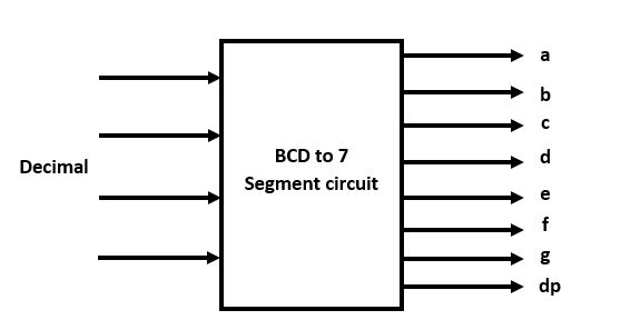
As the input to our BCD to the 7 segment block, we give a 4-bit binary number (0-9) which represents our BCD input. When the BCD is given to the circuit it generates an 8-bit signal where each bit signals to on or off our 8 segments in the 7 segment display.
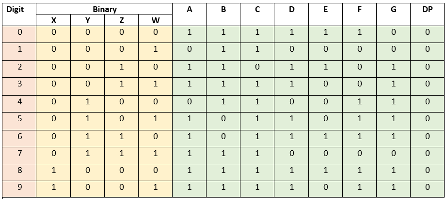
To implement this circuit first we need to write down the truth table and simplify the logic of each segment. Luckily it is explained thoroughly in a previous block. Click here to know more.
Creating our circuit using Verilog
Before we start, I should tell you there are 3 ways to create this circuit thanks to different coding styles in Verilog. For this, I will use 2 such ways.
- Gate Level Modelling – We have to code the circuit using logic gates.
- Behavioral Modelling – Coding the circuit using how it should behave.
It doesn’t matter which coding style you prefer but its a good practice to have a hierarchal approach when you code your design using hardware descriptive languages. So here, I follow a hierarchal approach to design my circuit. Because of that, I will mainly need 2 types of files.
- A top level file – We connect the small modules we created in this file.
- A low level file – This file describes the content inside our module.
From here onwards, lets dive into creating our circuit in Verilog.
Design using Gate Level Modelling
When we choose to design our circuit using gate-level modeling, it means that basically we have to use logic gates to implement our circuit. In order to do so, we need to obtain the logical expressions derived using basic logic gates for each of our 8 outputs from the BCD to 7 Segment block. Click here to see how it is deduced.
For convenience, I will summarize the expressions for our 8 outputs from our BCD to 7 segment block.
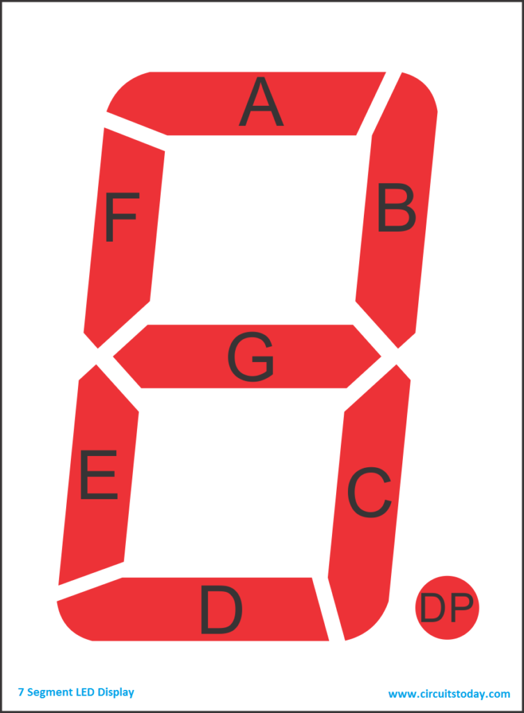
A = ~(In3) * ~(In2) * ~(In1) * (In0) + ~(In3) * (In2) * ~(In1) * ~(In0)B = ~(In3) * ~(In2) * ~(In1) * (In0) + ~(In3) * (In2) * ~(In1) * ~(In0)C = ~(In3) * ~(In2) * (In1) * ~(In0)D = ~(In3) * ~(In2) * ~(In1) * (In0) + ~(In3) * (In2) * ~(In1) * ~(In0)
+ ~(In3) * (In2) * (In1) * (In0)E = ~(In3) * (In0) + ~(In3) * (In2) * ~(In1) + ~(In2) * ~(In1) * (In0)F = ~(In3) * ~(In2) * (In0) + ~(In3) * ~(In2) * (In1) + ~(In3) * (In1) * (In0)G = ~(In3) * ~(In2) * ~(In1) + ~(In3) * (In2) * (In1) * (In0) DP = 1The next step is to describe the circuit using Verilog.
// This code is implements a BCD to 7-Segment Decoder using verilog
// We have used Hierarchical Design to implement our circuit
// This code creates a module called bcd7segment using Structural modeling (Gate-level design) which implements the BCD to 7-Segment Decoder
// This module is then initialized on the top level file
// All the deductions for the 7-segment display segments can be read on the link below
// https://focuslk.com/design-of-bcd-to-7-segment-display-decoder-using-logic-gates/

//Declaring the module
module bcd7segment(
	bcd,
	seg
	);

	input [3:0] bcd; //initializing bcd as an 4 bit input signal
	output[7:0] seg; //initializing seg as an 8 bit output signal

	wire [7:0] seg; //initializing bcd signal as wires

	assign seg[0]= ((~bcd[3])&(~bcd[2])&(~bcd[1])&bcd[0]) | ((~bcd[3])&bcd[2]&(~bcd[1])&(~bcd[0])); //Logical expression for segment0 (Segment A)

	assign seg[1]= ((~bcd[3])&bcd[2]&(~bcd[1])&bcd[0]) | ((~bcd[3])&bcd[2]&bcd[1]&(~bcd[0])); //Logical expression for segment1 (Segment B)

	assign seg[2]= ((~bcd[3])&(~bcd[2])&bcd[1]&(~bcd[0])); //Logical expression for segment2 (Segment C)

	assign seg[3] = ((~bcd[3])&(~bcd[2])&(~bcd[1])&bcd[0]) | ((~bcd[3])&bcd[2]&(~bcd[1])&(~bcd[0])) | ((~bcd[3])&bcd[2]&bcd[1]&bcd[0]); //Logical expression for segment3 (Segment D)

	assign seg[4] = ((~bcd[3])&bcd[0]) | ((~bcd[3])&bcd[2]&(~bcd[1])) | (~(bcd[2])&(~bcd[1])&bcd[0]); //Logical expression for segment4 (Segment E)

	assign seg[5] = ((~bcd[3])&(~bcd[2])&bcd[0]) | ((~bcd[3])&(~bcd[2])&bcd[1]) | ((~bcd[3])&bcd[1]&bcd[0]); //Logical expression for segment5 (Segment F)

	assign seg[6] = ((~bcd[3])&(~bcd[2])&(~bcd[1]))|((~bcd[3])&bcd[2]&bcd[1]&bcd[0]); //Logical expression for segment6 (Segment G)

	assign seg[7] = 1; //Logical expression for segment7 (Segment Decimal Point)
	endmodule

BCD-to-7-SEGMENT-using-Verilog- (this link opens in a new window) by pahanmendis (this link opens in a new window)
This repository contains verilog code used to implment a BCD to 7 segment display. This implementation is done using gate level modeling as well as behavioral modelling.
Design using Behevioral Modelling
Writing code using behavioral modeling is the easiest and far less frustrating. When we use this method for coding, we will get use of the @Always block. This block tells the Verilog synthesizer to create a circuit that evaluates our defined cases each and every time the value of BCD changes. When the BCD value changes it will choose the correct condition and assign the corresponding 8-bit hex value will be assigned to the output. We can take advantage of the truth table we deduced in the previous blog to identify the bit pattern of the output hex value.
// This code is implements a BCD to 7-Segment Decoder using verilog
// We have used Hierarchical Design to implement our circuit
// This code creates a module called bcd7segment using Behavioral modeling which implements the BCD to 7-Segment Decoder
// This module is then initialized on the top level file
// All the deductions for the 7-segment display segments can be read on the link below
// https://focuslk.com/design-of-bcd-to-7-segment-display-decoder-using-logic-gates/

//declaring the model
module bcd7segmentBehavioral(
			bcd,
			seg
			);
	input [3:0] bcd; 	//initializing bcd as an 4 bit input signal
	output[7:0] seg; 	//initializing seg as an 8 bit output signal
	reg [7:0] seg; 		//initializing bcd signal as registers

	always @ (bcd) 		//using the always statement to indicate any change in the bcd signal results in evaluating the declared cases
	begin
		case(bcd)	//begining the case statement which evaluates the bcd value and assigns the appropriate contol signals to our 8bit output signal).
			0: seg = 8'b11000000;	//when bcd = 0
			1: seg = 8'b11111001;	//when bcd = 1
			2: seg = 8'b10100100;	//when bcd = 2
			3: seg = 8'b10110000;	//when bcd = 3
			4: seg = 8'b10011001;	//when bcd = 4
			5: seg = 8'b10010010;	//when bcd = 5
			6: seg = 8'b10000010;	//when bcd = 6
			7: seg = 8'b11111000;	//when bcd = 7
			8: seg = 8'b10000000;	//when bcd = 8
			9: seg = 8'b10010000;	//when bcd = 9
			default: seg=8'b11111111;	//any other value
		endcase
	end
	endmodule
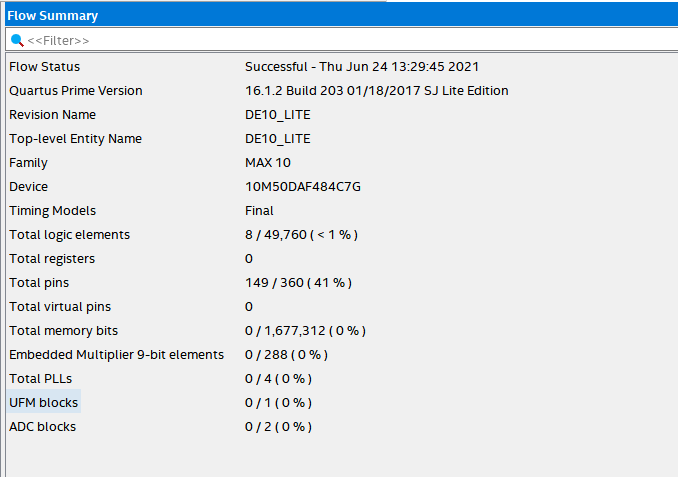
3. Creating the top-level file
At this stage we have already created our decoder. So now what is left is to connect the decoder to the inputs and outputs of our FPGA board. This will be done at the current stage.
To be clear of what we are doing, it’s always better to list down the connections somewhere before hand. For this circuit, I will do as follows.
- For the BCD input of the module, I will connect switches 0 to 3 which is addressed by SW[0] to SW[3].
- For the 7 bit output of the module, I will connect HEX0 which is the 0th seven segment display of our FPGA board.
Now let’s look at the Verilog implementation
//=======================================================
//  This is the top level file
//=======================================================

// This code is implements a BCD to 7-Segment Decoder using verilog
// We have used Hierarchical Design to implement our circuit
// This is the top level file
// The bcd7segment module is initialized by giving the proper signals
// All the deductions for the 7-segment display segments can be read on the link below
// https://focuslk.com/design-of-bcd-to-7-segment-display-decoder-using-logic-gates/


//=======================================================
//  This code is generated by Terasic System Builder
//=======================================================

module DE10_LITE_TOP(

	//////////// CLOCK //////////
	input 		          		ADC_CLK_10,
	input 		          		MAX10_CLK1_50,
	input 		          		MAX10_CLK2_50,

	//////////// SDRAM //////////
	output		    [12:0]		DRAM_ADDR,
	output		     [1:0]		DRAM_BA,
	output		          		DRAM_CAS_N,
	output		          		DRAM_CKE,
	output		          		DRAM_CLK,
	output		          		DRAM_CS_N,
	inout 		    [15:0]		DRAM_DQ,
	output		          		DRAM_LDQM,
	output		          		DRAM_RAS_N,
	output		          		DRAM_UDQM,
	output		          		DRAM_WE_N,

	//////////// SEG7 //////////
	output		     [7:0]		HEX0,
	output		     [7:0]		HEX1,
	output		     [7:0]		HEX2,
	output		     [7:0]		HEX3,
	output		     [7:0]		HEX4,
	output		     [7:0]		HEX5,

	//////////// KEY //////////
	input 		     [1:0]		KEY,

	//////////// LED //////////
	output		     [9:0]		LEDR,

	//////////// SW //////////
	input 		     [9:0]		SW,

	//////////// VGA //////////
	output		     [3:0]		VGA_B,
	output		     [3:0]		VGA_G,
	output		          		VGA_HS,
	output		     [3:0]		VGA_R,
	output		          		VGA_VS,

	//////////// Accelerometer //////////
	output		          		GSENSOR_CS_N,
	input 		     [2:1]		GSENSOR_INT,
	output		          		GSENSOR_SCLK,
	inout 		          		GSENSOR_SDI,
	inout 		          		GSENSOR_SDO,

	//////////// Arduino //////////
	inout 		    [15:0]		ARDUINO_IO,
	inout 		          		ARDUINO_RESET_N
);


//=======================================================
//  Structural coding
//=======================================================

//we need 4 inputs as the BCD - We take switches 0 to 4 in our Terrasic DE-10 lite
//we need 8 bit output for the display - We select Hex display 0 as out diplay

bcd7segment bcdCircuit(SW[3:0],HEX0);  //Making an instance of the BCD to 7 segment decoder

//uncomment this to run the circuit using behavioral modelling
//bcd7segmentBehavioral bcdCircuit1(SW[3:0],HEX0); //Making an instance of the BCD to 7 segment decoder


endmodule